
This is the multi-page printable view of this section. Click here to print.
konsool hardware
- 1: Konsool specifications
- 1.1: Konsool battery
- 1.2: Konsool ESP-C6
- 1.3: Konsool ESP-P4
- 1.4: Konsool keyboard
- 1.5: Konsool screen
- 2: Camera
- 3: Konsool connectors
- 4: Konsool pinouts
- 4.1: Konsool connectors
- 4.1.1: CATT pinout
- 4.1.2: QWIIC pinout
- 4.1.3: Internal expansion port
- 4.2: IC pinouts
- 4.2.1: CH32V203 pinout
- 4.2.2: ESP32C6 pinout
- 4.2.3: ESP32-P4 pinout
- 5: Frontpanel
- 5.1: Konsool artwork
1 - Konsool specifications
1.1 - Konsool battery
Battery

Specifications
| label | Value |
|---|---|
| Brand | Tewaycell |
| Type | Lithium ion |
| Voltage | 3.7V |
| Capacity | 2500 mAH (9.25Wh) |
1.2 - Konsool ESP-C6
Specifications
| label | Value |
|---|---|
| Type | ESP32-C6-WROOM-1 |
| Architecture | RISC-V |
| Flash | 8 mb |
| WIFI version | 6 |
| WIFI frequency | 2.4 GHz |
| Bluetooth | LE |
| IOT | Zigbee + THread (802.15.4) |
Datasheet
For detailed specifications please look at the datasheet
1.3 - Konsool ESP-P4
#Specifications
| label | Value |
|---|---|
| Type | ESP32-P4 |
| PSRAM | 16/32 mb |
| Architecture | RISC-V |
| High speed cores | 2 |
| High speed clock | 400MHz |
| Low speed cores | 1 |
| Low speed clock | 40 MHz |
For more details please look at the datasheet
1.4 - Konsool keyboard
#Specifications
QWERTY dome keyboard by Arturo
1.5 - Konsool screen
2 - Camera
Camera Compatibility List
| Camera | Sensor | Connector | Lens | “Night vision” | Flashlight | Autofocus | Tested |
|---|---|---|---|---|---|---|---|
| Camera Module for Raspberry Pi Zero | OV5647 | 22 pin Pi Zero/5 style | 120 degree fixed | No | No | No | No |
| Camera Module for Raspberry Pi Zero | OV5647 | 22 pin Pi Zero/5 style | 72 degree fixed | Yes | No | No | No |
| Camera Module for Raspberry Pi Zero | OV5647 | 22 pin Pi Zero/5 style | 72 degree fixed | No | No | No | No |
| Camera Module for Raspberry Pi Zero | OV5647 | 22 pin Pi Zero/5 style | 160 degree fixed | No | No | No | No |
| Camera Module for Raspberry Pi Zero | OV5647 | 22 pin Pi Zero/5 style | 120 degree fixed (big lens) | No | No | No | No |
| Camera Module for Raspberry Pi Zero | OV5647 | 22 pin Pi Zero/5 style | 120 degree motorized | No | No | Yes | No |
| Camera Module for Raspberry Pi Zero | OV5647 | 22 pin Pi Zero/5 style | 72 degree motorized | No | No | Yes | No |
| Raspberry Pi 5 camera | OV5647 | Comes with cable to 22 pin Pi Zero/5 style | FF 69 | No | No | No | No |
| Raspberry Pi 5 camera | OV5647 | Comes with cable to 22 pin Pi Zero/5 style | AF 65" | No | No | Yes | No |
| Raspberry Pi 5 camera | OV5647 | Comes with cable to 22 pin Pi Zero/5 style | IR-CUT 175 2 | Yes | IR | No | No |
| Raspberry Pi 5 camera | OV5647 | Comes with cable to 22 pin Pi Zero/5 style | IR-CUT 175 | Yes | No | No | No |
| Raspberry Pi 5 camera | OV5647 | Comes with cable to 22 pin Pi Zero/5 style | IR-CUT 75 2" | Yes | IR | No | No |
| Raspberry Pi 5 camera | OV5647 | Comes with cable to 22 pin Pi Zero/5 style | IR-CUT 75 | Yes | No | No | No |
| Raspberry Pi 5 camera | OV5647 | Comes with cable to 22 pin Pi Zero/5 style | MF 220 | No | No | No | No |
| Raspberry Pi 5 camera | OV5647 | Comes with cable to 22 pin Pi Zero/5 style | MF 175 | No | No | No | No |
| Raspberry Pi 5 camera | OV5647 | Comes with cable to 22 pin Pi Zero/5 style | MF 130 Night 2 | Yes | IR | No | No |
Not compatible
The new IMX519 based camera modules from Raspberry Pi are currently not supported. For a list of supported sensors see supported sensors.
| Camera | Sensor | Connector | Lens | “Night vision” | Flashlight | Autofocus |
|---|---|---|---|---|---|---|
| Raspberry Pi 5 camera | IMX519 | Comes with cable to 22 pin Pi Zero/5 style | Unknown | No | No | Yes |
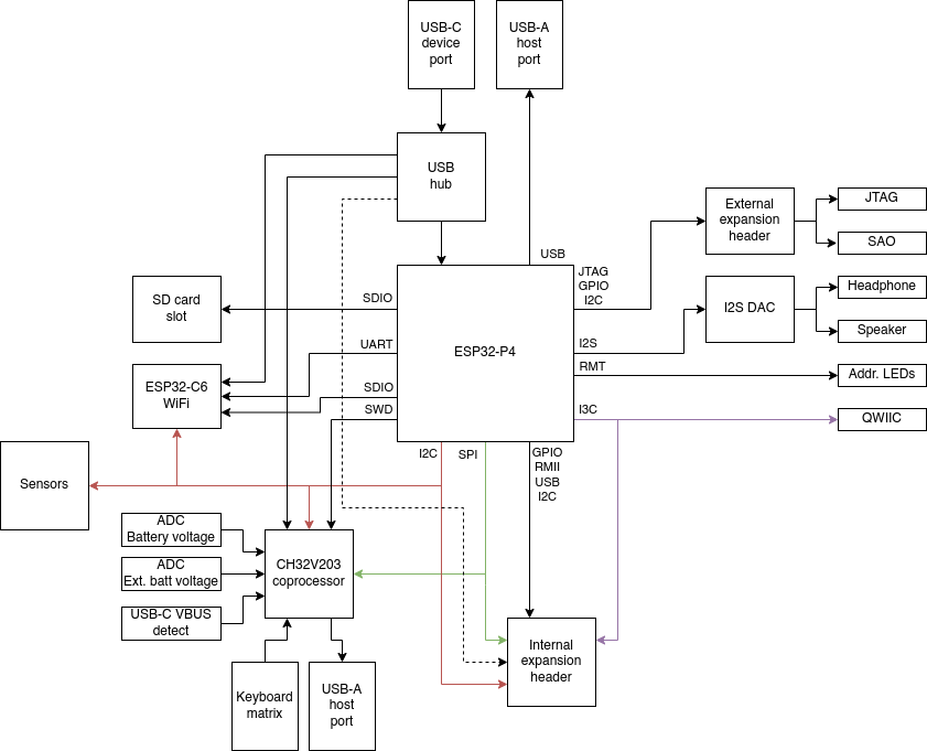
3 - Konsool connectors
Diagram
4 - Konsool pinouts
In this section you can find the pinout of the chips and connectors of the device.
4.1 - Konsool connectors
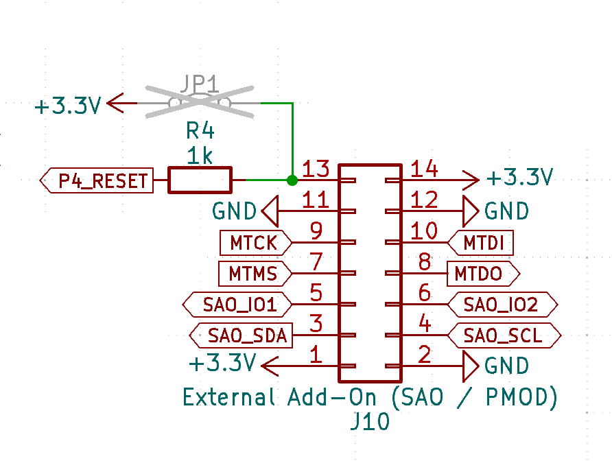
4.1.1 - CATT pinout
Description
The CATT connector combines several different connectors in one.
- Special Addon (SAO)
- JTAG
- PMOD
Because of this multi functional nature, the name for the connector is CATT (Connect all the things), even though there are more kind of things to connect.
SAO

- *DET: Detect, when pulled down during power up, JTAG functionality is provided
- *3V3: Not connected by default, jumper on the PCB needs to be closed to supply 3V3
Schematic
4.1.2 - QWIIC pinout
Description
The QWIIC connector combines I2C and I3C in one connector. Information about this connector and all of it’s versatile uses can be found on https://www.sparkfun.com/qwiic
For this connector sparkfun advices to use the standard cable so all modules you connect to this connector will work without any issues.

4.1.3 - Internal expansion port
Back Expansion layout

Back expansion port
This port is not exposed by default, and a modified back cover needs to be used to make it accessible. For this reason the port is also named the “internal expansion port”.
| Function | Name | GPIO | Description | Notes |
|---|---|---|---|---|
| Power output | VOTG | - | Output from booster DC/DC converter in the PMIC | 5 volt when booster is enabled, +/- VSYS when booster is disabled |
| USB | HUB_USB1_P | - | Port on USB hub for USB-C port (DP) | Can be used to expose an USB device on the add-on to the PC plugged into the USB-C port |
| Power output | HUB_USB1_N | - | Port on USB hub for USB-C port (DN) | Can be used to expose an USB device on the add-on to the PC plugged into the USB-C port |
| USB | VBATT | - | Battery voltage (3.0 – 4.2v) | Directly connected to battery connector, always on even when the device is turned off |
| Power output | VSYS | - | System voltage (3.0 – 5.0v) | Switched power rail for powering the system, can be powered by battery or USB-C port, off when device is turned off |
| Power ref. | GND | - | Voltage reference (ground) | |
| Power ref. | GND | - | Voltage reference (ground) | |
| Power output | +3.3v | - | Main logic supply rail (3.3v) | |
| I2C | INT_SCL | Internal I2C bus, shared with other I2C devices (SCL) | Used to connect I2C devices and an EEPROM for add-on identification | |
| I2C | INT_SDA | Internal I2C bus, shared with other I2C devices (SDA) | Used to connect I2C devices and an EEPROM for add-on identification | |
| GPIO | E0 | 36 | GPIO | |
| GPIO | E1 | 0 | GPIO | |
| GPIO | E2 | 6 | GPIO, also connected to camera GPIO 1 | Shared with camera connector |
| GPIO | E3 | 46 | GPIO, VSDCARD LDO must be enabled to use this pin | Connected via level shifter, externally these GPIOs operate at 3.3v but the GPIOs are powered by the VSDCARD power domain |
| GPIO | E4 | 47 | GPIO, VSDCARD LDO must be enabled to use this pin | Connected via level shifter, externally these GPIOs operate at 3.3v but the GPIOs are powered by the VSDCARD power domain |
| GPIO | E5 | 48 | GPIO, VSDCARD LDO must be enabled to use this pin | Connected via level shifter, externally these GPIOs operate at 3.3v but the GPIOs are powered by the VSDCARD power domain |
| GPIO | E6 | 45 | GPIO, VSDCARD LDO must be enabled to use this pin | Connected via level shifter, externally these GPIOs operate at 3.3v but the GPIOs are powered by the VSDCARD power domain |
| GPIO | E7 | 7 | GPIO, in low power domain of P4, has 51k pull-up resistor | Can be used as wakeup pin to wake up the ESP32-P4 from deep sleep |
| GPIO | E8 | 54 | GPIO | |
| GPIO | E9 | 49 | GPIO | |
| GPIO | E10 | 53 | GPIO | |
| GPIO | EXT_USB_P | 26 | Can be used as GPIO or as USB FS PHY (DP) | The USB PHYs of the P4 can be swapped between the USB serial/jtag and user controlled USB peripheral. If badgelink is used then this PHY exposes the serial/jtag peripheral |
| GPIO | E11 | 52 | GPIO | |
| GPIO | EXT_USB_N | 27 | Can be used as GPIO or as USB FS PHY (DN) | The USB PHYs of the P4 can be swapped between the USB serial/jtag and user controlled USB peripheral. If badgelink is used then this PHY exposes the serial/jtag peripheral |
| GPIO | E12 | 51 | GPIO | |
| GPIO | P4_TX | 37 | Exposes boot console of P4, can be used as GPIO | Must be low during boot |
| GPIO | E13 | 50 | GPIO | |
| GPIO | P4_RX | 38 | Exposes boot console of P4, can be used as GPIO | Must be high during boot |
| I2S | I2S_MCLK | Digital audio bus master clock | Reference clock for connected I2S devices | |
| I2S | I2S_LRCK | Digital audio bus word clock | Word clock (left-right selection) for connected I2S devices | |
| I2S | I2S_DATA | Digital audio bus data output | Data output from mainboard for connected I2S DACs | |
| I2S | I2S_SCLK | Digital audio bus sample clock | Sample clock for connected I2S devices | |
| Power output | +3.3v | - | Main logic supply rail (3.3v) | |
| I3C | I3C_SDA | I3C bus, shared with QWIIC connector (SDA) | Can also be used as I2C bus | |
| Power ref. | GND | - | Voltage reference (ground) | |
| I3C | I3C_SCL | I3C bus, shared with QWIIC connector (SCL) | Can also be used as I2C bus |
Limitations & warnings
- Total for all 3.3v outputs must not exceed 1A of current. It is generally adviced to stay well below this figure.
- Do not exceed a current of 1.5A from the battery when the battery is connected to the internal battery connector
- Do not charge the battery via the internal add-on port
4.2 - IC pinouts
IC pinout mapping to functions on the board.
4.2.1 - CH32V203 pinout
CH32V203

| Pin Number | Pin Name | Net Name | Direction | Notes |
|---|---|---|---|---|
| 1 | VBAT | VBAT | Power | Regulated 2.5V supply |
| 2 | PC13 | POWER_ON_PULSE | Output | Emit pulse to wake up badge |
| 3 | PC14 | XTAL | Input | Crystal Oscillator |
| 4 | PC15 | XTAL | Input | Crystal Oscillator |
| 5 | PD0 | AMP_EN | Output | Enable audio speaker amplifier |
| 6 | PD1 | USB_ENABLE | Output | Enable to USB-A OTG port |
| 7 | NRST | NRST | Input | 3V3 |
| 8 | VSSA | VSSA | Power | Analog Ground |
| 9 | VDDA | VDDA | Power | Analog Power |
| 10 | PA0 | INT | Output | Interrupt line to ESP32-P4 |
| 11 | PA1 | KB_ROW5 | Output | Keyboard IO |
| 12 | PA2 | KB_ROW8 | Output | Keyboard IO |
| 13 | PA3 | KB_ROW4 | Output | Keyboard IO |
| 14 | PA4 | KB_ROW3 | Output | Keyboard IO |
| 15 | PA5 | KB_ROW7 | Output | Keyboard IO |
| 16 | PA6 | KB_ROW6 | Output | Keyboard IO |
| 17 | PA7 | KB_COL3 | Input | Keyboard IO |
| 18 | PB0 | KB_COL7 | Input | Keyboard IO |
| 19 | PB1 | KB_COL2 | Input | Keyboard IO |
| 20 | PB2/BOOT1 | KB_COL6 | Input | Keyboard IO |
| 21 | PB10 | PM_SCL | Output | I2C Clock PMIC (Power controller) |
| 22 | PB11 | PM_SDA | Bidirectional | I2C Data PMIC |
| 23 | VSS1 | GND | Power | Ground |
| 24 | VDDIO1 | +3.3V | Power | Power Supply |
| 25 | PB12 | KB_COL1 | Input | Keyboard IO |
| 26 | PB13 | KB_COL5 | Input | Keyboard IO |
| 27 | PB14 | KB_COL0 | Input | Keyboard IO |
| 28 | PB15 | KB_COL4 | Input | Keyboard IO |
| 29 | PA8 | KB_ROW0 | Output | Keyboard IO |
| 30 | PA9 | KB_ROW1 | Output | Keyboard IO |
| 31 | PA10 | KB_ROW2 | Output | Keyboard IO |
| 32 | PA11 | LED_DATA | Output | Serial data to SK6805 LEDs |
| 33 | PA12 | POWER_BTN | Input | Power button input (low when pressed) |
| 34 | PA13 | SWDIO | Bidirectional | Debug Interface CH32V203 |
| 35 | VSS2 | GND | Power | Ground |
| 36 | VDD2 | +3.3V | Power | Power Supply |
| 37 | PA14 | SWCLK | Output | Debug Clock |
| 38 | PA15 | SD_DET | Input | SD card detect |
| 39 | PB3 | KEYBOARD_BL | Output | Enable backlight Keyboard |
| 40 | PB4 | DISPLAY_BL | Output | Enable backlight display |
| 41 | PB5 | HP_DET | Input | Head phone detect |
| 42 | PB6 | SCL | input | I2C Clock shared bus |
| 43 | PB7 | SDA | Bidirectional | I2C Data shared bus |
| 44 | BOOT0 | DCAM_IO0 | Output | Camera module power enable (if present) |
| 45 | PB8 | RADIO_ENABLE / CAM_IO0 | Output | Enable C6 and MIPI_CSI camera IO 0 |
| 46 | PB9 | PM_INT | Input | Interrupt signal PMIC |
| 47 | VSS3 | GND | Power | GND |
| 48 | VDDIO3 | +3.3V | Power | Power |
4.2.2 - ESP32C6 pinout
Schematic

ESP32 Pin table
| Pin | Name | Net | Direction | Function |
|---|---|---|---|---|
| 1 | GND | Power | ||
| 2 | 3V3 | Power | ||
| 3 | EN | EN | Input | Enable signal from the CH32V203 |
| 4 | IO4 | LORA_DIO1 | Input | LoRa IRQ (Interrupt) |
| 5 | IO5 | LORA_BUSY | Input | LoRa Busy Signal |
| 6 | IO6 | I2C_SDA | Bidirectional | I2C Data Line |
| 7 | IO7 | I2C_SCL | Input | I2C Clock Line |
| 8 | IO0 | LORA_SCK | Input | LoRa SPI Clock |
| 9 | IO1 | LORA_CS | Output | LoRa SPI Chip Select |
| 10 | IO8 | INT | Output | Interrupt line to ESP32-P4 |
| 11 | IO10 | LORA_RESET | Output | LoRa Reset |
| 12 | GND | Power | ||
| 13 | IO12 | C6_USB1_N | Bidirectional | Via USB hub to USB-C port |
| 14 | IO13 | C6_USB1_P | Bidirectional | Via USB hub to USB-C port |
| 15 | IO9 | BOOT | Input | BOOT mode select and VUSB (USB-A power) enable line |
| 16 | IO18 | SDIO_CMD | Bidirectional | SDIO bus to P4 Command |
| 17 | IO19 | SDIO_CLK | Output | SDIO bus to P4 Clock |
| 18 | IO20 | SDIO_DATA0 | Bidirectional | SDIO bus to P4 Data Line 0 |
| 19 | IO21 | SDIO_DATA1 | Bidirectional | SDIO bus to P4 Data Line 1 |
| 20 | IO22 | SDIO_DATA2 | Bidirectional | SDIO bus to P4 Data Line 2 |
| 21 | IO23 | SDIO_DATA3 | Bidirectional | SDIO bus to P4 Data Line 3 |
| 22 | NC | |||
| 23 | IO15 | IR_LED | Output | Infrared LED Control |
| 24 | RXD0 | RX | Input | UART to P4 Receive |
| 25 | TXD0 | TX | Output | UART to P4 Transmit |
| 26 | IO3 | LORA_MISO | Input | LoRa SPI MISO |
| 27 | IO2 | LORA_MOSI | Output | LoRa SPI MOSI |
| 28 | GND | Power | ||
| 29 | GND | Power |
4.2.3 - ESP32-P4 pinout
ESP32-P4 (U8)
LDO
| Pin number | Pin name | Pin net |
|---|---|---|
| 71 | VFB/VO1 | VFLASH |
| 72 | VFB/VO2 | VPSRAM |
| 73 | VFB/VO3 | VMIPI |
| 74 | VFB/VO4 | VSDCARD |
GPIO
| GPIO | Direction / Bus | Function | Note |
|---|---|---|---|
| 0 | User controlled | Internal Add-On: E2 | |
| 1 | Input | Interrupt from CH32V203 coprocessor | High on interrupt from CH32 co-processor |
| 2 | User controlled | JTAG: MTCK, PMOD: IO | Can be used as JTAG interface or as generic GPIO on the external Add-On connector |
| 3 | User controlled | JTAG: MTDI, PMOD: IO | Can be used as JTAG interface or as generic GPIO on the external Add-On connector |
| 4 | User controlled | JTAG: MTMS, PMOD: IO | Can be used as JTAG interface or as generic GPIO on the external Add-On connector |
| 5 | User controlled | JTAG: MTDO, PMOD: IO | Can be used as JTAG interface or as generic GPIO on the external Add-On connector |
| 6 | Input | E1 expansion + Camera module LED enable | Read from the coprocessor I2C device to clear the interrupt condition |
| 7 | Input / User controlled | Interrupt from internal Add-On board | Can also be used as GPIO, depending on the needs of the internal Add-On board |
| 8 | Input | Interrupt from ESP32-C6 radio | Controlled by ESP-HOSTED component |
| 9 | I2C bus SDA | Internal I2C bus data | Internal I2C bus connecting the ESP32-P4 to the ESP32-C6, CH32V203 coprocessor, Bosch sensors and internal Add-On board |
| 10 | I2C bus SCL | Internal I2C bus clock | Internal I2C bus connecting the ESP32-P4 to the ESP32-C6, CH32V203 coprocessor, Bosch sensors and internal Add-On board |
| 11 | Input | LCD TE (Tearing effect) | Synchronization pin for frame sync, used to avoid tearing |
| 12 | User controlled | SAO: I2C SDA, PMOD: IO | Can be used as I2C interface for SAO Add-On boards or as generic GPIO on the external Add-On connector |
| 13 | User controlled | SAO: I2C SCL, PMOD: IO | Can be used as I2C interface for SAO Add-On boards or as generic GPIO on the external Add-On connector |
| 14 | Output | LCD reset | Hardware reset for the LCD controller |
| 15 | User controlled | SAO: IO1, PMOD: IO | Can be used as generic GPIO for SAO Add-On boards or as generic GPIO on the external Add-On connector |
| 16 | SDIO 2.0 | SDIO bus for ESP32-C6: CMD | Controlled by ESP-HOSTED component |
| 17 | SDIO 2.0 | SDIO bus for ESP32-C6: CLK | Controlled by ESP-HOSTED component |
| 18 | SDIO 2.0 | SDIO bus for ESP32-C6: D0 | Controlled by ESP-HOSTED component |
| 19 | SDIO 2.0 | SDIO bus for ESP32-C6: D1 | Controlled by ESP-HOSTED component |
| 20 | SDIO 2.0 | SDIO bus for ESP32-C6: D2 | Controlled by ESP-HOSTED component |
| 21 | SDIO 2.0 | SDIO bus for ESP32-C6: D3 | Controlled by ESP-HOSTED component |
| 22 | Bidirectional | CH32V203 programming interface: SWDIO | For coprocessor firmware updates |
| 23 | Output | CH32V203 programming interface: SWCLK | For coprocessor firmware updates |
| 24 | USB | USB DN, port 1 on USB hub (USB-C port) | |
| 25 | USB | USB DP, port 1 on USB hub (USB-C port) | |
| 26 | User controlled | Internal Add-On: USB DN or generic GPIO | Pin 24 |
| 27 | User controlled | Internal Add-On: USB DP or generic GPIO | Pin 22 |
| 28 | I2S | I2S: data | Internal I2S to the DAC towards headphone jack and speaker |
| 29 | I2S | I2S: sample clock | Internal I2S to the DAC towards headphone jack and speaker |
| 30 | I2S | I2S: master clock | Internal I2S to the DAC towards headphone jack and speaker |
| 31 | I2S | I2S: lr clock | Internal I2S to the DAC towards headphone jack and speaker |
| 32 | I3C | I2C/I3C QWIIC port: SCL | Connected to external I3C connector |
| 33 | I3C | I2C/I3C QWIIC port: SDA | Connected to external I3C connector |
| 34 | User controlled | SAO: IO2, PMOD: IO | |
| 35 | User controlled | Internal Add-On: E1 / BOOT | 1 during reset release SPI boot, 0 is DEBUG (page 32 data sheet) (Connected up to volume down button) |
| 36 | User controlled | Internal Add-On: E0 | Depending on fuses can influence boot |
| 37 | Output / User controlled | Debug UART transmit | Pin 26 on the back expansion |
| 38 | Input / User controlled | Debug UART receive | Pin 28 on the back expansion |
| 39 | SDIO 3.0 | SD card slot: D0 | |
| 40 | SDIO 3.0 | SD card slot: D1 | |
| 41 | SDIO 3.0 | SD card slot: D2 | |
| 42 | SDIO 3.0 | SD card slot: D3 | |
| 43 | SDIO 3.0 | SD card slot: CLK | |
| 44 | SDIO 3.0 | SD card slot: CMD | |
| 45 | User controlled | Internal Add-On: E6 | Pin 17 Back expansion header |
| 46 | User controlled | Internal Add-On: E3 | Pin 14 Back expansion header |
| 47 | User controlled | Internal Add-On: E4 | Pin 15 Back expansion header |
| 48 | User controlled | Internal Add-On: E5 | Pin 16 Back expansion header |
| 49 | User controlled | Internal Add-On: E7 | Pin 20 Back expansion header |
| 50 | User controlled | Internal Add-On: E8 | Pin 27 Back expansion header |
| 51 | User controlled | Internal Add-On: E9 | Pin 25 Back expansion header |
| 52 | User controlled | Internal Add-On: E10 | Pin 23 Back expansion header |
| 53 | User controlled | Internal Add-On: E11 | Pin 21 Back expansion header |
| 54 | User controlled | Internal Add-On: E12 | Pin 19 Back expansion header |
5 - Frontpanel
This page describes how to design and order a Konsool badge frontpanel.
Designing a frontpanel using Inkscape, svg2shenzhen and KiCad
The first step of designing a frontpanel is creating artwork that can be converted into a KiCad footprint. For this Inkscape and the Inkscape plugin svg2shenzhen are used.
Of course it is also possible to use any other method which allows you to import a footprint into KiCad so if you’re using a different method then you can skip ahead to the KiCad section.
Instructions on how to install svg2shenzhen can be found in the readme of the repository.
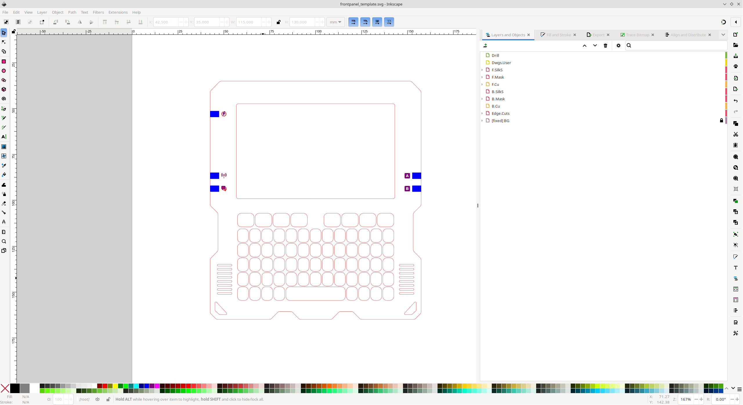
After opening the design file in Inkscape you will notice that multiple layers are used. Each of the layers in the design corresponds with a KiCad layer, this allows you to define how a shape should appear on the circuit board.
The most important layers are:
- Edge.Cuts: this is the outline of the board, the PCB manufacturer will use a CNC mill to cut the board following the edges of the object on this layer.
- F.Cu and B.Cu: these layers define where to place copper on the front and back of the circuit board.
- F.Mask and B.Mask: all shapes drawn on this layer are cut out of the colored soldermask layer of the board.
- F.SilkS and B.SilkS: these layers are printed on the front and back silkscreen layer respectively. The silkscreen layer is a non-conductive layer of ink usually used to add reference designators and text to a circuit board.
Mask layer
The mask layers are negative layers, the contents of the layer determine where NOT to place soldermask.Silkscreen
Silkscreen can only be placed on top of solder mask, silkscreen overlapping with any area defined in the mask layers will be removed by the board manufacturer. Keep in mind that KiCad will render the silkscreen in these locations but that this does not match the end result.Edge cut
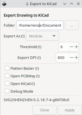
Round shapes are not correctly exported to KiCad on the Edge.Cuts layer. Workaround is adding a lot more nodes and preferably setting segments to be straight.Export the design to KiCad by navigating to Extensions > Svg2Shenzhen > 2. Export to Kicad...
KiCad
…