In this section you can find the pinout of the chips and connectors of the device.
This is the multi-page printable view of this section. Click here to print.
Konsool pinouts
- 1: Konsool connectors
- 1.1: CATT pinout
- 1.2: QWIIC pinout
- 1.3: Internal expansion port
- 2: IC pinouts
- 2.1: CH32V203 pinout
- 2.2: ESP32C6 pinout
- 2.3: ESP32-P4 pinout
1 - Konsool connectors
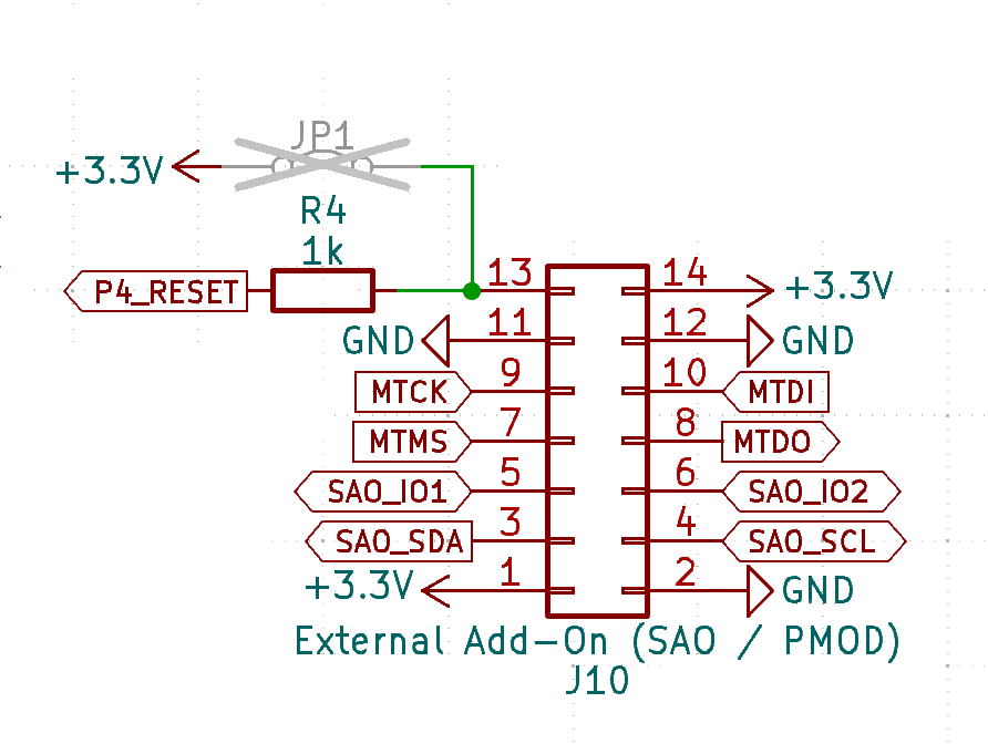
1.1 - CATT pinout
Description
The CATT connector combines several different connectors in one.
- Special Addon (SAO)
- JTAG
- PMOD
Because of this multi functional nature, the name for the connector is CATT (Connect all the things), even though there are more kind of things to connect.
SAO

- *DET: Detect, when pulled down during power up, JTAG functionality is provided
- *3V3: Not connected by default, jumper on the PCB needs to be closed to supply 3V3
Schematic
1.2 - QWIIC pinout
Description
The QWIIC connector combines I2C and I3C in one connector. Information about this connector and all of it’s versatile uses can be found on https://www.sparkfun.com/qwiic
For this connector sparkfun advices to use the standard cable so all modules you connect to this connector will work without any issues.

1.3 - Internal expansion port
Back Expansion layout

Back expansion port
This port is not exposed by default, and a modified back cover needs to be used to make it accessible. For this reason the port is also named the “internal expansion port”.
| Function | Name | GPIO | Description | Notes |
|---|---|---|---|---|
| Power output | VOTG | - | Output from booster DC/DC converter in the PMIC | 5 volt when booster is enabled, +/- VSYS when booster is disabled |
| USB | HUB_USB1_P | - | Port on USB hub for USB-C port (DP) | Can be used to expose an USB device on the add-on to the PC plugged into the USB-C port |
| Power output | HUB_USB1_N | - | Port on USB hub for USB-C port (DN) | Can be used to expose an USB device on the add-on to the PC plugged into the USB-C port |
| USB | VBATT | - | Battery voltage (3.0 – 4.2v) | Directly connected to battery connector, always on even when the device is turned off |
| Power output | VSYS | - | System voltage (3.0 – 5.0v) | Switched power rail for powering the system, can be powered by battery or USB-C port, off when device is turned off |
| Power ref. | GND | - | Voltage reference (ground) | |
| Power ref. | GND | - | Voltage reference (ground) | |
| Power output | +3.3v | - | Main logic supply rail (3.3v) | |
| I2C | INT_SCL | Internal I2C bus, shared with other I2C devices (SCL) | Used to connect I2C devices and an EEPROM for add-on identification | |
| I2C | INT_SDA | Internal I2C bus, shared with other I2C devices (SDA) | Used to connect I2C devices and an EEPROM for add-on identification | |
| GPIO | E0 | 36 | GPIO | |
| GPIO | E1 | 0 | GPIO | |
| GPIO | E2 | 6 | GPIO, also connected to camera GPIO 1 | Shared with camera connector |
| GPIO | E3 | 46 | GPIO, VSDCARD LDO must be enabled to use this pin | Connected via level shifter, externally these GPIOs operate at 3.3v but the GPIOs are powered by the VSDCARD power domain |
| GPIO | E4 | 47 | GPIO, VSDCARD LDO must be enabled to use this pin | Connected via level shifter, externally these GPIOs operate at 3.3v but the GPIOs are powered by the VSDCARD power domain |
| GPIO | E5 | 48 | GPIO, VSDCARD LDO must be enabled to use this pin | Connected via level shifter, externally these GPIOs operate at 3.3v but the GPIOs are powered by the VSDCARD power domain |
| GPIO | E6 | 45 | GPIO, VSDCARD LDO must be enabled to use this pin | Connected via level shifter, externally these GPIOs operate at 3.3v but the GPIOs are powered by the VSDCARD power domain |
| GPIO | E7 | 7 | GPIO, in low power domain of P4, has 51k pull-up resistor | Can be used as wakeup pin to wake up the ESP32-P4 from deep sleep |
| GPIO | E8 | 54 | GPIO | |
| GPIO | E9 | 49 | GPIO | |
| GPIO | E10 | 53 | GPIO | |
| GPIO | EXT_USB_P | 26 | Can be used as GPIO or as USB FS PHY (DP) | The USB PHYs of the P4 can be swapped between the USB serial/jtag and user controlled USB peripheral. If badgelink is used then this PHY exposes the serial/jtag peripheral |
| GPIO | E11 | 52 | GPIO | |
| GPIO | EXT_USB_N | 27 | Can be used as GPIO or as USB FS PHY (DN) | The USB PHYs of the P4 can be swapped between the USB serial/jtag and user controlled USB peripheral. If badgelink is used then this PHY exposes the serial/jtag peripheral |
| GPIO | E12 | 51 | GPIO | |
| GPIO | P4_TX | 37 | Exposes boot console of P4, can be used as GPIO | Must be low during boot |
| GPIO | E13 | 50 | GPIO | |
| GPIO | P4_RX | 38 | Exposes boot console of P4, can be used as GPIO | Must be high during boot |
| I2S | I2S_MCLK | Digital audio bus master clock | Reference clock for connected I2S devices | |
| I2S | I2S_LRCK | Digital audio bus word clock | Word clock (left-right selection) for connected I2S devices | |
| I2S | I2S_DATA | Digital audio bus data output | Data output from mainboard for connected I2S DACs | |
| I2S | I2S_SCLK | Digital audio bus sample clock | Sample clock for connected I2S devices | |
| Power output | +3.3v | - | Main logic supply rail (3.3v) | |
| I3C | I3C_SDA | I3C bus, shared with QWIIC connector (SDA) | Can also be used as I2C bus | |
| Power ref. | GND | - | Voltage reference (ground) | |
| I3C | I3C_SCL | I3C bus, shared with QWIIC connector (SCL) | Can also be used as I2C bus |
Limitations & warnings
- Total for all 3.3v outputs must not exceed 1A of current. It is generally adviced to stay well below this figure.
- Do not exceed a current of 1.5A from the battery when the battery is connected to the internal battery connector
- Do not charge the battery via the internal add-on port
2 - IC pinouts
IC pinout mapping to functions on the board.
2.1 - CH32V203 pinout
CH32V203

| Pin Number | Pin Name | Net Name | Direction | Notes |
|---|---|---|---|---|
| 1 | VBAT | VBAT | Power | Regulated 2.5V supply |
| 2 | PC13 | POWER_ON_PULSE | Output | Emit pulse to wake up badge |
| 3 | PC14 | XTAL | Input | Crystal Oscillator |
| 4 | PC15 | XTAL | Input | Crystal Oscillator |
| 5 | PD0 | AMP_EN | Output | Enable audio speaker amplifier |
| 6 | PD1 | USB_ENABLE | Output | Enable to USB-A OTG port |
| 7 | NRST | NRST | Input | 3V3 |
| 8 | VSSA | VSSA | Power | Analog Ground |
| 9 | VDDA | VDDA | Power | Analog Power |
| 10 | PA0 | INT | Output | Interrupt line to ESP32-P4 |
| 11 | PA1 | KB_ROW5 | Output | Keyboard IO |
| 12 | PA2 | KB_ROW8 | Output | Keyboard IO |
| 13 | PA3 | KB_ROW4 | Output | Keyboard IO |
| 14 | PA4 | KB_ROW3 | Output | Keyboard IO |
| 15 | PA5 | KB_ROW7 | Output | Keyboard IO |
| 16 | PA6 | KB_ROW6 | Output | Keyboard IO |
| 17 | PA7 | KB_COL3 | Input | Keyboard IO |
| 18 | PB0 | KB_COL7 | Input | Keyboard IO |
| 19 | PB1 | KB_COL2 | Input | Keyboard IO |
| 20 | PB2/BOOT1 | KB_COL6 | Input | Keyboard IO |
| 21 | PB10 | PM_SCL | Output | I2C Clock PMIC (Power controller) |
| 22 | PB11 | PM_SDA | Bidirectional | I2C Data PMIC |
| 23 | VSS1 | GND | Power | Ground |
| 24 | VDDIO1 | +3.3V | Power | Power Supply |
| 25 | PB12 | KB_COL1 | Input | Keyboard IO |
| 26 | PB13 | KB_COL5 | Input | Keyboard IO |
| 27 | PB14 | KB_COL0 | Input | Keyboard IO |
| 28 | PB15 | KB_COL4 | Input | Keyboard IO |
| 29 | PA8 | KB_ROW0 | Output | Keyboard IO |
| 30 | PA9 | KB_ROW1 | Output | Keyboard IO |
| 31 | PA10 | KB_ROW2 | Output | Keyboard IO |
| 32 | PA11 | LED_DATA | Output | Serial data to SK6805 LEDs |
| 33 | PA12 | POWER_BTN | Input | Power button input (low when pressed) |
| 34 | PA13 | SWDIO | Bidirectional | Debug Interface CH32V203 |
| 35 | VSS2 | GND | Power | Ground |
| 36 | VDD2 | +3.3V | Power | Power Supply |
| 37 | PA14 | SWCLK | Output | Debug Clock |
| 38 | PA15 | SD_DET | Input | SD card detect |
| 39 | PB3 | KEYBOARD_BL | Output | Enable backlight Keyboard |
| 40 | PB4 | DISPLAY_BL | Output | Enable backlight display |
| 41 | PB5 | HP_DET | Input | Head phone detect |
| 42 | PB6 | SCL | input | I2C Clock shared bus |
| 43 | PB7 | SDA | Bidirectional | I2C Data shared bus |
| 44 | BOOT0 | DCAM_IO0 | Output | Camera module power enable (if present) |
| 45 | PB8 | RADIO_ENABLE / CAM_IO0 | Output | Enable C6 and MIPI_CSI camera IO 0 |
| 46 | PB9 | PM_INT | Input | Interrupt signal PMIC |
| 47 | VSS3 | GND | Power | GND |
| 48 | VDDIO3 | +3.3V | Power | Power |
2.2 - ESP32C6 pinout
Schematic

ESP32 Pin table
| Pin | Name | Net | Direction | Function |
|---|---|---|---|---|
| 1 | GND | Power | ||
| 2 | 3V3 | Power | ||
| 3 | EN | EN | Input | Enable signal from the CH32V203 |
| 4 | IO4 | LORA_DIO1 | Input | LoRa IRQ (Interrupt) |
| 5 | IO5 | LORA_BUSY | Input | LoRa Busy Signal |
| 6 | IO6 | I2C_SDA | Bidirectional | I2C Data Line |
| 7 | IO7 | I2C_SCL | Input | I2C Clock Line |
| 8 | IO0 | LORA_SCK | Input | LoRa SPI Clock |
| 9 | IO1 | LORA_CS | Output | LoRa SPI Chip Select |
| 10 | IO8 | INT | Output | Interrupt line to ESP32-P4 |
| 11 | IO10 | LORA_RESET | Output | LoRa Reset |
| 12 | GND | Power | ||
| 13 | IO12 | C6_USB1_N | Bidirectional | Via USB hub to USB-C port |
| 14 | IO13 | C6_USB1_P | Bidirectional | Via USB hub to USB-C port |
| 15 | IO9 | BOOT | Input | BOOT mode select and VUSB (USB-A power) enable line |
| 16 | IO18 | SDIO_CMD | Bidirectional | SDIO bus to P4 Command |
| 17 | IO19 | SDIO_CLK | Output | SDIO bus to P4 Clock |
| 18 | IO20 | SDIO_DATA0 | Bidirectional | SDIO bus to P4 Data Line 0 |
| 19 | IO21 | SDIO_DATA1 | Bidirectional | SDIO bus to P4 Data Line 1 |
| 20 | IO22 | SDIO_DATA2 | Bidirectional | SDIO bus to P4 Data Line 2 |
| 21 | IO23 | SDIO_DATA3 | Bidirectional | SDIO bus to P4 Data Line 3 |
| 22 | NC | |||
| 23 | IO15 | IR_LED | Output | Infrared LED Control |
| 24 | RXD0 | RX | Input | UART to P4 Receive |
| 25 | TXD0 | TX | Output | UART to P4 Transmit |
| 26 | IO3 | LORA_MISO | Input | LoRa SPI MISO |
| 27 | IO2 | LORA_MOSI | Output | LoRa SPI MOSI |
| 28 | GND | Power | ||
| 29 | GND | Power |
2.3 - ESP32-P4 pinout
ESP32-P4 (U8)
LDO
| Pin number | Pin name | Pin net |
|---|---|---|
| 71 | VFB/VO1 | VFLASH |
| 72 | VFB/VO2 | VPSRAM |
| 73 | VFB/VO3 | VMIPI |
| 74 | VFB/VO4 | VSDCARD |
GPIO
| GPIO | Direction / Bus | Function | Note |
|---|---|---|---|
| 0 | User controlled | Internal Add-On: E2 | |
| 1 | Input | Interrupt from CH32V203 coprocessor | High on interrupt from CH32 co-processor |
| 2 | User controlled | JTAG: MTCK, PMOD: IO | Can be used as JTAG interface or as generic GPIO on the external Add-On connector |
| 3 | User controlled | JTAG: MTDI, PMOD: IO | Can be used as JTAG interface or as generic GPIO on the external Add-On connector |
| 4 | User controlled | JTAG: MTMS, PMOD: IO | Can be used as JTAG interface or as generic GPIO on the external Add-On connector |
| 5 | User controlled | JTAG: MTDO, PMOD: IO | Can be used as JTAG interface or as generic GPIO on the external Add-On connector |
| 6 | Input | E1 expansion + Camera module LED enable | Read from the coprocessor I2C device to clear the interrupt condition |
| 7 | Input / User controlled | Interrupt from internal Add-On board | Can also be used as GPIO, depending on the needs of the internal Add-On board |
| 8 | Input | Interrupt from ESP32-C6 radio | Controlled by ESP-HOSTED component |
| 9 | I2C bus SDA | Internal I2C bus data | Internal I2C bus connecting the ESP32-P4 to the ESP32-C6, CH32V203 coprocessor, Bosch sensors and internal Add-On board |
| 10 | I2C bus SCL | Internal I2C bus clock | Internal I2C bus connecting the ESP32-P4 to the ESP32-C6, CH32V203 coprocessor, Bosch sensors and internal Add-On board |
| 11 | Input | LCD TE (Tearing effect) | Synchronization pin for frame sync, used to avoid tearing |
| 12 | User controlled | SAO: I2C SDA, PMOD: IO | Can be used as I2C interface for SAO Add-On boards or as generic GPIO on the external Add-On connector |
| 13 | User controlled | SAO: I2C SCL, PMOD: IO | Can be used as I2C interface for SAO Add-On boards or as generic GPIO on the external Add-On connector |
| 14 | Output | LCD reset | Hardware reset for the LCD controller |
| 15 | User controlled | SAO: IO1, PMOD: IO | Can be used as generic GPIO for SAO Add-On boards or as generic GPIO on the external Add-On connector |
| 16 | SDIO 2.0 | SDIO bus for ESP32-C6: CMD | Controlled by ESP-HOSTED component |
| 17 | SDIO 2.0 | SDIO bus for ESP32-C6: CLK | Controlled by ESP-HOSTED component |
| 18 | SDIO 2.0 | SDIO bus for ESP32-C6: D0 | Controlled by ESP-HOSTED component |
| 19 | SDIO 2.0 | SDIO bus for ESP32-C6: D1 | Controlled by ESP-HOSTED component |
| 20 | SDIO 2.0 | SDIO bus for ESP32-C6: D2 | Controlled by ESP-HOSTED component |
| 21 | SDIO 2.0 | SDIO bus for ESP32-C6: D3 | Controlled by ESP-HOSTED component |
| 22 | Bidirectional | CH32V203 programming interface: SWDIO | For coprocessor firmware updates |
| 23 | Output | CH32V203 programming interface: SWCLK | For coprocessor firmware updates |
| 24 | USB | USB DN, port 1 on USB hub (USB-C port) | |
| 25 | USB | USB DP, port 1 on USB hub (USB-C port) | |
| 26 | User controlled | Internal Add-On: USB DN or generic GPIO | Pin 24 |
| 27 | User controlled | Internal Add-On: USB DP or generic GPIO | Pin 22 |
| 28 | I2S | I2S: data | Internal I2S to the DAC towards headphone jack and speaker |
| 29 | I2S | I2S: sample clock | Internal I2S to the DAC towards headphone jack and speaker |
| 30 | I2S | I2S: master clock | Internal I2S to the DAC towards headphone jack and speaker |
| 31 | I2S | I2S: lr clock | Internal I2S to the DAC towards headphone jack and speaker |
| 32 | I3C | I2C/I3C QWIIC port: SCL | Connected to external I3C connector |
| 33 | I3C | I2C/I3C QWIIC port: SDA | Connected to external I3C connector |
| 34 | User controlled | SAO: IO2, PMOD: IO | |
| 35 | User controlled | Internal Add-On: E1 / BOOT | 1 during reset release SPI boot, 0 is DEBUG (page 32 data sheet) (Connected up to volume down button) |
| 36 | User controlled | Internal Add-On: E0 | Depending on fuses can influence boot |
| 37 | Output / User controlled | Debug UART transmit | Pin 26 on the back expansion |
| 38 | Input / User controlled | Debug UART receive | Pin 28 on the back expansion |
| 39 | SDIO 3.0 | SD card slot: D0 | |
| 40 | SDIO 3.0 | SD card slot: D1 | |
| 41 | SDIO 3.0 | SD card slot: D2 | |
| 42 | SDIO 3.0 | SD card slot: D3 | |
| 43 | SDIO 3.0 | SD card slot: CLK | |
| 44 | SDIO 3.0 | SD card slot: CMD | |
| 45 | User controlled | Internal Add-On: E6 | Pin 17 Back expansion header |
| 46 | User controlled | Internal Add-On: E3 | Pin 14 Back expansion header |
| 47 | User controlled | Internal Add-On: E4 | Pin 15 Back expansion header |
| 48 | User controlled | Internal Add-On: E5 | Pin 16 Back expansion header |
| 49 | User controlled | Internal Add-On: E7 | Pin 20 Back expansion header |
| 50 | User controlled | Internal Add-On: E8 | Pin 27 Back expansion header |
| 51 | User controlled | Internal Add-On: E9 | Pin 25 Back expansion header |
| 52 | User controlled | Internal Add-On: E10 | Pin 23 Back expansion header |
| 53 | User controlled | Internal Add-On: E11 | Pin 21 Back expansion header |
| 54 | User controlled | Internal Add-On: E12 | Pin 19 Back expansion header |