MCH2022 Badge Hardware
Block diagram
The badge contains a huge amount of awesome chips, so many that a block
diagram is necessary to explain how everything is interconnected.
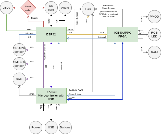
The ESP32 is at the center of the operation. It has access to almost all
the peripherals on the badge and using its WiFi connectivity it can
load new firmware and applications from the internet.
The RP2040 microcontroller provides USB connectivity consisting of two
serial ports (for the ESP32 and the FPGA), WebUSB for managing the badge
using your browser and HID for acting like a keyboard, mouse or
joystick. It also drives the SK6812-EC15 addressable LEDs, giving the
badge a lot of bling and eyecandy. To top it off a lot of the I/O pins
of the RP2040 have been broken out, both as the IO pins of the SAO
connector and as testpads next to the prototyping areas on the back of
the badge.
The ICE40UP5K FPGA is programmed over an SPI connection by the ESP32.
Using this connection the FPGA can also communicate with the application
running on the ESP32. Our goal is to enable people to learn about HDL
programming so new bitstreams can easily be loaded into the FPGA by user
applications, to provide any function you want ranging from a simple LED
blinker to a RISC-V SoC. To accomodate more advanced designs the FPGA is
connected to the LCD display via a parallel bus, enabling it to update
the display at high refresh rates, as well as 8MB of PSRAM via a
Quad-SPI bus. 8 of the I/O pins of the FPGA have been broken out as an
industry standard PMOD header, allowing users to connect standard
expansion modules or their own creations.
Resources
Datasheets and Resources
- ESP32 datasheet the datasheet for the main processor
- ESP32 technical reference technical reference for the main processor. This contains information about the features of the chip, so technically, it belongs in the firmware section, but … whatever.
- WROVER datasheet datasheet of the module. The processor is packed together with peripherals necessary for operations in a module (WROVER) nuder a metallic can.
- RP2040 documentation site and datasheet
- Lattice ICE40UP5K - iCE40UltraPlus documentation site and datasheet
- BME680 4 in 1 gas sensor. (temperature, humidity, air pressure and volatile organic compounds (VOC)
- BNO055 accelerometer, gyroscope, magnetometer sensor
- Display also have a look here
- SK6812-EC15 addressable RGB - LEDs (aka Neopixel)
- MS4344 Audio DAC
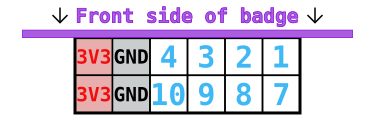
1 - MCH2022 badge pinouts
Connectors
SAO (Shitty AddOn)
Addon connector following the SHITTY ADD-ON V1.69BIS standard.
| Pin | Description | Direction | Connection |
|---|
| 1 | VCC | Power output | 3.3v supply voltage output |
| 2 | GND | Power output | Ground reference |
| 3 | SDA | Data IO | I2C bus data |
| 4 | SCL | Data output | I2C bus clock |
| 5 | GPIO1 | Data IO | User configurable IO, connected to RP2040 GPIO18 |
| 6 | GPIO2 | Data IO | User configurable IO, connected to RP2040 GPIO19 |
PMOD (peripheral module interface)
The PMOD connector is wired up to the iCE40 FPGA. Note that while the connector is physically located on the backside of the badge, it has been wired up such that the PMOD’s top side must be pointed in the same direction as the badge’s top.
| PMOD pin | ICE40 pin | Note |
|---|
| 1 | 47 | IOB_2a (paired with PMOD pin 7 IOB_3b_G6) |
| 2 | 48 | IOB_4a (paired with PMOD pin 8 IOB_5b) |
| 3 | 4 | IOB_8a (paired with PMOD pin 9 IOB_9b) |
| 4 | 2 | IOB_6a |
| 7 | 44 | IOB_3b_G6 (paired with PMOD pin 1 IOB_2a) |
| 8 | 45 | IOB_5b (paired with PMOD pin 2 IOB_4a) |
| 9 | 3 | IOB_9b (paired with PMOD pin 3 IOB_8a) |
| 10 | 46 | IOB_0a |
Chips
ESP32
| ESP32 GPIO | Direction | Function | Note |
|---|
| 0 | Both | I2S master clock output / UART download select input | Drives I2S DAC / driven by RP2040 through resistor |
| 1 | Output | UART TX | Connected to RP2040 |
| 2 | Both | SD card data 0 | SD card slot |
| 3 | Input | UART RX | Connected to RP2040 |
| 4 | Output | I2S bit clock | |
| 5 | Output | LED data | Connected to the SK6805 LEDs in the kite |
| 12 | Output | I2S LR channel select | |
| 13 | Output | I2S data | |
| 14 | Output | SD clock | SD card slot |
| 15 | Output | SD command | SD card slot |
| 18 | Output | SPI clock | Connected to LCD and FPGA |
| 19 | Output | SD card and kite LED power control | Set high to enable power to LEDs and SD card |
| 21 | Output | I2C clock | Connected to RP2040, BNO055, BME680, Qwiic connector and SAO addon connector |
| 22 | Both | I2C data | Connected to RP2040, BNO055, BME680, Qwiic connector and SAO addon connector |
| 23 | Output | SPI MOSI | Data from ESP32 to LCD / FPGA |
| 25 | Both | LCD reset | Set to output low to reset LCD, leave floating normally |
| 26 | Output | LCD mode | Low: LCD in SPI mode, high: LCD in parallel mode |
| 27 | Output | SPI chip select for ICE40 | Low: select ICE40, high: deselect ICE40 |
| 32 | Both | SPI chip select for LCD | Low: select LCD, high: deselect LCD. Note: output in LCD SPI mode, input in LCD parallel mode |
| 33 | Both | LCD DC (data or command) selection | Note: output in LCD SPI mode, input in LCD parallel mode |
| 34 | Input | Interrupt from RP2040 | |
| 35 | Input | SPI MISO | Connected to ICE40 |
| 36 (SENSOR_VP) | Input | Interrupt from position sensor (BNO055) | |
| 39 (SENSOR_VN) | Input | Interrupt from ICE40 FPGA | |
RP2040
| RP2040 GPIO | Direction | Pull | Function | Description |
|---|
| 0 | Output | | UART0 TX | ESP32 UART |
| 1 | Input | | UART0 RX | ESP32 UART |
| 2 | Both | | I2C1 SDA | I2C bus data (RP2040 is in slave mode) |
| 3 | Input | | I2C1 SCL | I2C bus clock |
| 4 | Input | Up | GPIO | Button: MENU |
| 5 | Input | Up | GPIO | Button: HOME |
| 6 | Input | Up | GPIO | Button: ACCEPT |
| 7 | Input | Up | GPIO | Button: Joystick A |
| 8 | Input | Up | GPIO | Button: Joystick B |
| 9 | Input | Up | GPIO | Button: Joystick C |
| 10 | Input | Up | GPIO | Button: Joystick D |
| 11 | Input | Up | GPIO | Button: Joystick E |
| 12 | Both | | GPIO | ESP32 bootloader mode¹ |
| 13 | Output | | GPIO | ESP32 enable |
| 14 | Both | | GPIO | ESP32 interrupt¹ |
| 15 | Output | | PWM | LCD backlight brightness |
| 16 | Both | | GPIO | Available next to prototyping area |
| 17 | Both | | GPIO | Available next to prototyping area |
| 18 | Both | | GPIO | SAO GPIO1 |
| 19 | Both | | GPIO | SAO GPIO2 |
| 20 | Input | | GPIO | FPGA done |
| 21 | Output | | GPIO | FPGA reset |
| 22 | Input | Up | GPIO | Button: START |
| 23 | Input | | GPIO | LiPo charger state |
| 24 | Output | | UART1 TX | FPGA UART |
| 25 | Input | | UART1 RX | FPGA UART |
| 26 | Input | Up | GPIO | Button: BACK |
| 27 | Output | | GPIO | Infrared LED |
| 28 | Input | | ADC | Voltage measurement: USB input |
| 29 | Input | | ADC | Voltage measurement: Battery |
¹: Set to input normally and force low to activate
ICE40 FPGA
| ICE40 pin | ICE40 GPIO | Direction | Description | Notes |
|---|
| 2 | IOB_6a | Both | PMOD pin 4 | |
| 3 | IOB_8a | Both | PMOD pin 3 | |
| 4 | IOB_9b | Both | PMOD pin 9 | |
| 6 | IOB_13b | Input | UART RX | |
| 9 | IOB_16a | Output | UART TX | |
| 10 | IOB_18a | Output | Interrupt | Active-low |
| 11 | IOB_20a | Output | LCD register select | |
| 12 | IOB_22b | Both | RAM SPI D2 | |
| 13 | IOB_24a | Both | RAM SPI D1 | |
| 14 | IOB_32a_SPI_SO | Output | SPI MISO | |
| 15 | IOB_34b_SPI_SCK | Input | SPI SCK | |
| 16 | IOB_35b_SPI_SS | Input | SPI SS | |
| 17 | IOB_33b_SPI_SI | Input | SPI MOSI | |
| 18 | IOB_31b | Output | RAM SPI CS | |
| 19 | IOB_29b | Output | RAM SPI SCK | |
| 20 | IOB_25b_G3 | Both | RAM SPI D3 | |
| 21 | IOB_23b | Both | RAM SPI D0 | |
| 23 | IOT_37a | Output | LCD write | |
| 25 | IOT_36b | Input | LCD frame sync | |
| 26 | IOT_39a | Output | LCD data 0 | |
| 27 | IOT_38a | Output | LCD data 1 | |
| 28 | IOT_41a | Output | LCD CS | |
| 31 | IOT_42b | Output | LCD data 2 | |
| 32 | IOT_43a | Output | LCD data 3 | |
| 34 | IOT_44b | Output | LCD data 4 | |
| 35 | IOT_46b_G0 | Input | 12MHz clock | |
| 36 | IOT_48b | Output | LCD reset | Active-low, drive open-drain |
| 37 | IOT_45a_G1 | Output | LCD data 5 | |
| 38 | IOT_50b | Output | LCD data 6 | |
| 39 | RGB0 | Output | LED | |
| 40 | RGB1 | Output | LED | |
| 41 | RGB2 | Output | LED | |
| 42 | IOT_51a | Output | LCD data 7 | |
| 43 | IOT_49a | Input | LCD mode | Should be driven by ESP and monitored by FPGA |
| 44 | IOB_3b_G6 | Both | PMOD pin 7 | |
| 45 | IOB_5b | Both | PMOD pin 8 | |
| 46 | IOB_0a | Both | PMOD pin 10 | |
| 47 | IOB_2a | Both | PMOD pin 1 | |
| 48 | IOB_4a | Both | PMOD pin 2 | |
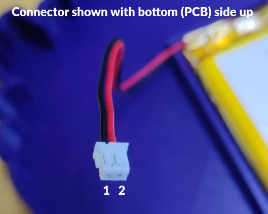
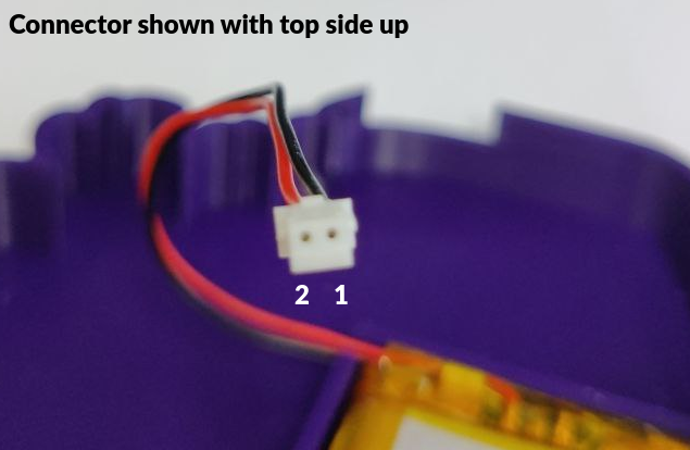
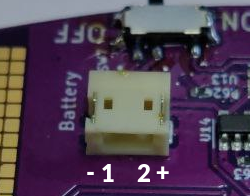
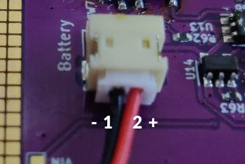
2 - Battery
The MCH2022 badge uses the JST S2B-ZR-SM4A-TF connector for the battery. This connector has two pins at 1.5mm pitch.
Pinout
| Pin | Function | Wire color |
|---|
| 1 | GND | Black |
| 2 | Vbatt | Red |
Photos
3 - MCH2022 Badge Hardware Hacking
The badge is made for hacking, and the hardware is no exception. There are several intended ways to extend the badge, next to unlimited unintented ones.
If you have access to a 3D printer, an easy and worthwile hardware mod is to
print a knob for the joystick, such as this
one or a case.
Shitty Add-on
The badge has a SAO header,
which can provide power, I2C, and 2 GPIOs to small accessories that can be plugged in.
Qwiic
At the back of the badge there is a Qwiic connector hooked up to the ESP32 that is compatible with a large family of modules from Sparkfun, Adafruit and others.
PMOD
On the side of the badge there is a PMOD connector hooked up to the FPGA that is compatible with a large family of modules from Digilent and others.
May Contain Hardware Area
On the back of the badge there is a prototyping area with a grid of pads, as well as pads the expose I2C, power, and GPIOs.
Across the rest of the PCB are labeled pads that expose things like the LED serial data, audio signal, IR signal, various debug pads, and more.